Large-scale research facilities for advanced manufacturing and semiconductor technologies
The stations at the large-scale research facilities of the Paul Scherrer Institute PSI make it possible to research micro- and nanostructures and utilise corresponding structures for various applications. In-situ imaging processes and analytics enable the development and optimisation of additive manufacturing methods. The development of methods and processes for EUV lithography is another focus. The analytics technology transfer centre ANAXAM, which is also located in the park, uses the research infrastructure of the PSI and carries out very successful projects with industrial partners.
The basis and common denominator of many technologies and their industrial applications is materials science, which investigates how the internal structure and observable properties of different materials are linked. It creates important foundations for the development of new materials and applications. The following expertise is available to you on site:
- Advanced analyses
- Biomaterials
- Polymer technologies
- X-ray and optical extreme UV technologies
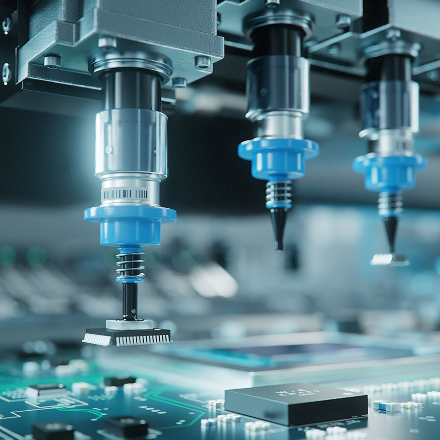
- Microfabrication and nanofabrication technologies
- Nanolithographic processes
Paul Scherrer Institute PSI
The large-scale research facilities of the Paul Scherrer Institute PSI make it possible to investigate micro- and nanostructures down to the molecular and atomic level as well as their functions - i.e. their dynamic and physical, chemical and biological properties and processes. The knowledge gained forms the basis for industrial innovations in the fields of energy, the environment, chemistry, pharmaceuticals, food, metallurgy and microelectronics.