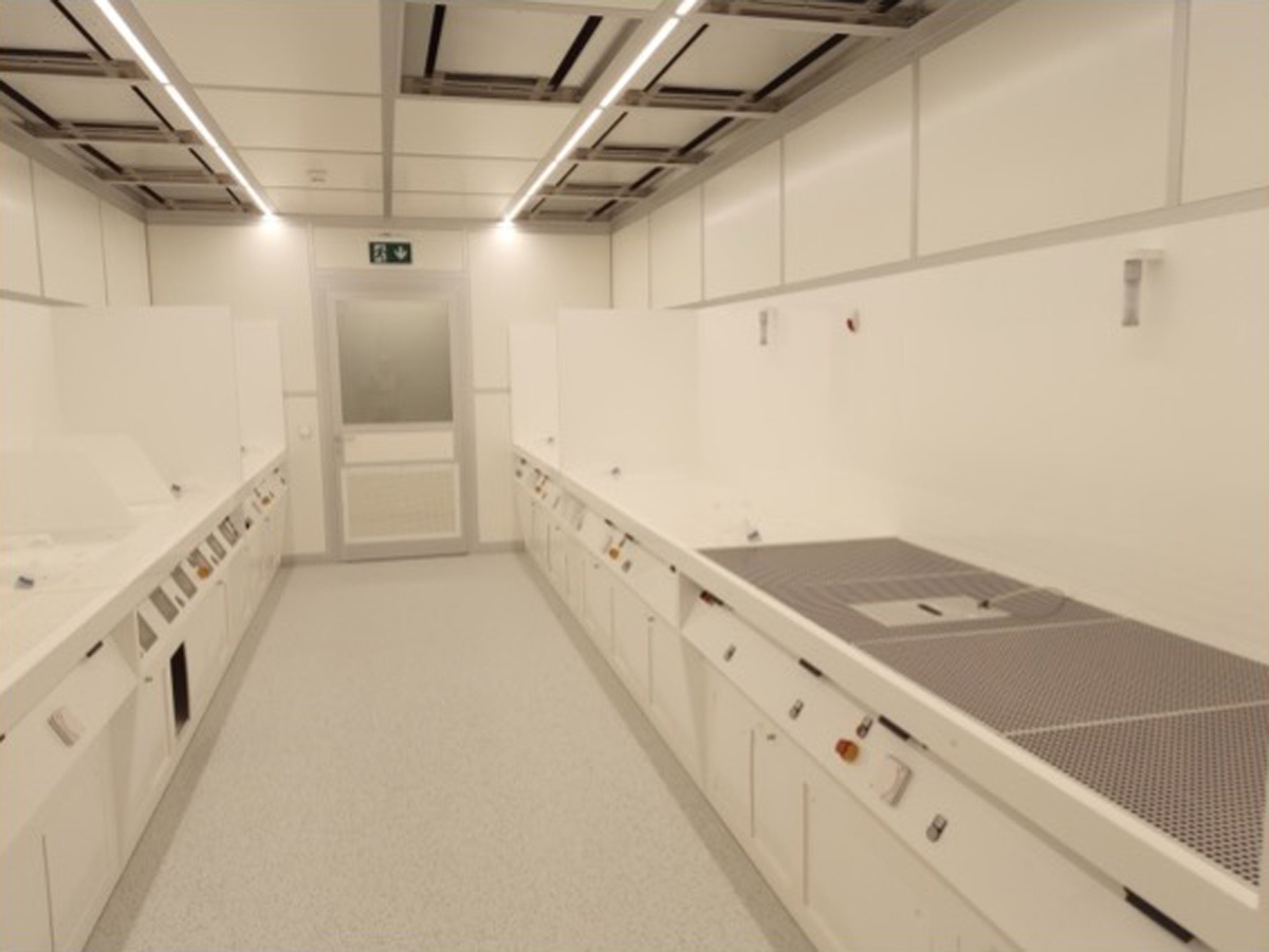
Ultramodern cleanrooms
Park Innovaare offers companies access to the Paul Scherrer Institute (PSI) nanofabrication cleanroom facility, as well as access to adjoining cleanroom or lab space, which they can fit out and customise for their own specific uses. Our innovation campus is the perfect location for existing science and technology companies looking to expand, or for start-ups and companies seeking an entrepreneurial platform for their projects. In addition to the cleanrooms, we also offer furnished biology, chemistry, physics, and analytics laboratories with basic equipment.
Cleanrooms PSI: Joint R&D projects
Companies on the Park Innovaare campus can collaborate with researchers of the Paul Scherrer Institute (PSI) in joint projects or as part of a service level agreement. High-tech firms working in the field of micro and nano fabrication, for example, can take advantage of the extensive know-how that scientists at the Paul Scherrer Institute (PSI) can offer in the areas of plasma etching, lithographic processes, thin film technology, electron microscopy, etc.
Special strength: The core value is the profound expertise held by our cadre of scientists, complemented by an array of cutting-edge technological tools at our disposal. In the realm of collaborative projects our state-of-the-art cleanroom facilities, alongside their adept specialists, furnish novel and extended capacities, exemplified by:
- From chip to 8-inch wafer capability
- State-of-the-art semiconductor fabrication capability
- Advanced lithography: two 100 kV E-Beams, grey-scale lithography, X-ray analysis
- Thin-film deposition and dry etching capability (metals and dielectrics)
- A wide range of characterization and metrology set-ups
- New tools that focus on quantum applications (superconducting films)
Improving, developing & refining processes
What we’d like to highlight: PSI’s highly advanced lithographic processes ranging from high-resolution E-beam to 3D structuring. As Professor Kirsten Moselund, Head of the Laboratory for Nano and Quantum Technologies that operates the cleanrooms at PSI, explains: “The usual lithography technique for making microchips is black and white, which means it is used to write a two-dimensional pattern. But now we can also create 3D structures, in a process known as grayscale lithography."
An important area of application for grayscale lithography for example is the modern micro-optics. Micro-optic systems are fitted in every tablet or smartphone as well. PSI also supports research in E-beam lithography and EUV resists.
PSI also offers a wide range of thin film deposition techniques for dielectrics and metals, along with associated dry- and wet-etching capability. Some of the differentiating factors when comparing with other cleanroom facilities in Switzerland is a focus on 8” wafer processing capability to enable industrial collaboration as well as processes and expertise dedicated to quantum technologies.
The key to success
What makes our clean room so successful is the choice of equipment!
Professor Kirsten Moselund: “Generally speaking, we welcome industrial partners to our cleanrooms – they can use the available tools under the same general conditions as all other users (permitted material classes and processes). We do not rent dedicated space in the PSI part of the cleanroom for companies to install their own equipment, but we are open to discussing the purchase of tools by companies, as long as they make them available to other users.”
Are you interested in projects with PSI scientists or cleanrooms in general? Please contact:info(at)parkinnovaare.ch

